September 2025
How Computers Work
From Logic Gates To Assembly
Hardware Foundation
Binary and Logic Gates
Everything in a computer begins at the hardware level with simple on/off switches. These two states represent 1 and 0, forming the foundation of binary. While seemingly basic, these switches can be combined to perform complex calculations.
Bits and Bytes
A single binary digit (0 or 1) is called a bit, which is the smallest unit of data in computing. Each bit represents one piece of information: on or off, true or false, high voltage or low voltage.
Eight bits grouped together form a byte, which is the fundamental unit of memory in most computer systems. A byte can represent 256 different values (2^8), from 0 to 255 in decimal, or 00000000 to 11111111 in binary.
Let's see how binary numbers work:
Bit positions:  7  6  5  4  3  2  1  0
Powers of 2:  128 64 32 16  8  4  2  1
Binary:         0  0  0  0  1  0  1  0
                            ↑     ↑
                            8  +  2  = 10 in decimal
Binary is a base-2 number system, meaning each bit position represents a power of 2. To convert binary to decimal, we add up the values where bits are set to 1. In the example above, bits 1 and 3 are set (reading from right to left, starting at position 0), giving us 2 + 8 = 10.
With 8 bits (one byte), we can represent:
- Numbers from 0 to 255 (unsigned)
- Numbers from -128 to 127 (signed, using two's complement)
- ASCII characters (like 'A' = 65, 'a' = 97)
- Instructions and opcodes for the CPU
- Colors, sounds, or any other data
The binary system is essential because it maps perfectly to the physical world of electronics: a high voltage represents a 1, and a low or no voltage represents a 0.
Logic Gates
Logic Gates are the fundamental building blocks of digital circuits. Each gate takes one or more binary inputs and produces a single, predictable binary output based on a specific logical operation.
The most common logic gates are:
- AND: Outputs 1 only if both inputs are 1
- OR: Outputs 1 if either input is 1
- NOT: Inverts the input (0 becomes 1, 1 becomes 0)
- XOR (Exclusive OR): Outputs 1 if inputs are different
When you chain logic gates together, you can create circuits that perform arithmetic operations. For example, an adder circuit can sum binary numbers.
Let's see a simple addition: 5 + 10 = 15
Binary addition:
    0101  (5)
  + 1010  (10)
  ------
    1111  (15)
The hardware works with their binary equivalents: 0101 (5) + 1010 (10) = 1111 (15). Inside the CPU, this addition happens through a combination of AND, OR, and XOR gates working together to handle each bit position and any carry-over to the next position.
CPU Architecture
So how do we get from simple binary math to a functioning computer? This is where the CPU comes in. Let's use the Nintendo Entertainment System (NES) MOS 6502 CPU as our example.
A CPU is connected to the rest of the computer through a series of physical pins. The 6502 has:
- An 8-bit data width: 8 pins used to send or receive data.
- A 16-bit address width: 16 pins used to specify a location in memory.
If we want to work with the number 10, the CPU places high voltage on the second and fourth data pins (D1 and D3) to represent its binary form, 00001010.
        +------------------------+
        |                        |
        |          CPU           |
        |                        |
        +------------------------+
          |  |  |  |  |  |  |  |
Pins:     D7 D6 D5 D4 D3 D2 D1 D0
          |  |  |  |  |  |  |  |
Binary:   0  0  0  0  1  0  1  0 = 10
          |  |  |  |  |  |  |  |
State:    ------------*-----*---
Similarly, to access memory address 32941, it places high voltage on the appropriate address pins to represent its binary form, 1000000010101101.
        +---------------------------------------------------------------+
        |                                                               |
        |                              CPU                              |
        |                                                               |
        +---------------------------------------------------------------+
          |   |   |   |   |   |   |   |   |   |   |   |   |   |   |   |
Pins:     A0  A1  A2  A3  A4  A5  A6  A7  A8  A9  A10 A11 A12 A13 A14 A15
          |   |   |   |   |   |   |   |   |   |   |   |   |   |   |   |
Binary:   1   0   1   1   0   1   0   1   0   0   0   0   0   0   0   1   = 32941
          |   |   |   |   |   |   |   |   |   |   |   |   |   |   |   |
State:    *-------*---*-------*-------*-------------------------------*
Memory and Addressing
With its 16 address pins, the CPU can specify 65,536 unique memory locations (from $0000 to $FFFF), each holding a single byte.
As numbers grow larger, reading long sequences of ones and zeros becomes impractical. This is why we use Hexadecimal as a more convenient shorthand. For example, the 16-bit binary address 1000000010101101 (decimal 32941) is simply $80AD in hex.
Hexadecimal works well because it aligns perfectly with binary (base-2). Each hexadecimal digit represents exactly four binary digits (bits). The system uses digits 0 through 9, and then the letters A through F to represent the decimal values 10 through 15.
Assembly
Instructions and Registers
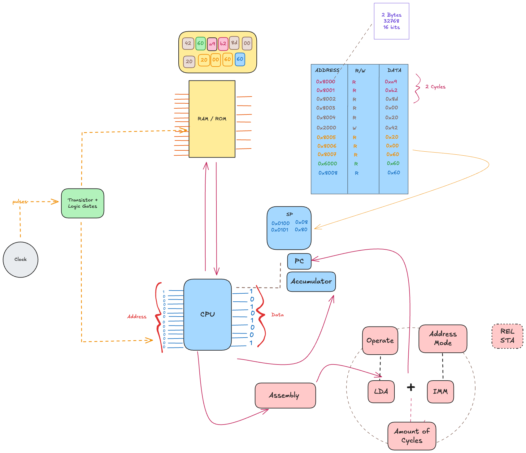
For the CPU to do anything useful, it must be given instructions. These instructions, represented by numbers called opcodes (and often operands), are stored in memory right alongside data. Data and instructions are stored together in memory as sequences of bytes. To keep everything synchronized, a Clock provides a steady pulse. On each tick of the clock, the CPU performs one step of an operation.
The CPU always knows which instruction to fetch next by consulting an internal pointer called the Program Counter (PC). Inside the CPU are also a few small, high-speed storage locations called Registers. You can think of them as the CPU's own global variables. The main registers in the 6502 are:
- The Accumulator (A), used for most arithmetic.
- Index Registers (X and Y), often used as counters or offsets.
- The Stack Pointer (SP), to manage a special memory area called the stack.
- The Status Register, which holds flags that report the outcome of operations (e.g., if the result was zero).
Addressing Modes
An instruction's behavior is determined by its addressing mode, which tells the CPU how to find the data it needs. The addressing mode used also affects how many clock cycles an instruction takes to execute.
The following operation loads the value $42 into the Accumulator, then adds the value stored at memory address $2000 to it:
| Address | Data | Action |
|---|---|---|
| $8000 | $A9 | Load the value $42 into Accumulator A. |
| $8001 | $42 | A = $42. |
| $8002 | $6D | Add with Carry from address $2000. |
| $8003 | $00 | Low-byte of the address. |
| $8004 | $20 | High-byte of the address. |
| $2000 | $10 | The data at address $2000 is $10. A = $52. |
This operation takes a total of 6 clock cycles to complete. Remembering the numeric opcodes ($A9, $6D) is difficult, so programmers write in human-readable assembly language. An Assembler tool then translates these instructions into the machine code the CPU understands.
LDA #$42
ADC $2000
The modes used in the example above are:
- Immediate (IMM) mode (
LDA #$42): The#tells the CPU the data it needs is the byte immediately following the instruction. - Absolute (ABS) mode (
ADC $2000): This tells the CPU the data is at a full 16-bit memory location, specified by the next two bytes.
Little-Endian and Multi-Byte Values
When the CPU needs to read a 16-bit address like $2000, it must do so in two steps since its data bus is only 8-bits wide. The 6502 uses Little-Endian byte ordering, meaning it reads the low-byte first, then the high-byte.
In the example above, when the assembler encounters ADC $2000, it stores the address in memory as:
- Address
$8003:$00(low-byte) - Address
$8004:$20(high-byte)
The CPU reads these bytes sequentially: first $00, then $20, reconstructing the full address $2000. This two-step read contributes to the instruction's total cycle count. Little-Endian ordering affects how all multi-byte data is stored and read in the 6502's memory.
Subroutines and the Stack
Programs aren't just a straight line of instructions. An instruction like JMP (Jump) changes the Program Counter directly, causing execution to "jump" to a new location.
An even more powerful instruction is JSR (Jump to Subroutine), which first saves the current location before jumping. Subroutines are the foundation of functions. This "return address" is pushed onto a special memory area called the Stack. The Stack is a "Last-In, First-Out" (LIFO) structure managed by the Stack Pointer. The stack resides in memory from $0100 to $01FF and grows downward (from $01FF toward $0100).
This table shows the 6 clock cycles JSR takes to execute:
| Cycles | PC | Data | Stack Address | Action |
|---|---|---|---|---|
| 1 | $8000 | $20 | $01FF | Fetch opcode (JSR) |
| 2 | $8001 | $15 | $01FF | Fetch low-byte of target address |
| 3 | $8002 | $40 | $01FF | Fetch high-byte of target address |
| 4 | $8002 | $80 | $01FF > $80 | Push high-byte of return address |
| 5 | $8002 | $02 | $01FE > $02 | Push low-byte of return address |
| 6 | $4015 | $40 | $01FD | Copy target address to PC |
When a subroutine is finished, it uses RTS (Return from Subroutine) to pull the return address off the stack and resume where it left off. If subroutines are called without returning, the stack will fill up and overwrite other parts of memory, causing a stack overflow.
This table shows the 6 clock cycles RTS takes to execute:
| Cycles | PC | Data | Stack Address | Action |
|---|---|---|---|---|
| 1 | $401A | $60 | $01FD | Fetch opcode (RTS) |
| 2 | $401B | $60 | $01FD | Internal operation |
| 3 | $401B | $60 | $01FE | Increment SP |
| 4 | $401B | $02 | $01FE < $02 | Pull low-byte of return address |
| 5 | $401B | $80 | $01FF < $80 | Pull high-byte of return address |
| 6 | $8003 | $?? | $01FF | Increment PC and continue |
These are expressed as assembly instructions:
JSR $4015

RTS
Preserving Register State
The stack isn't only for return addresses. It's also crucial for temporarily saving the state of the CPU's registers. Imagine a subroutine needs to use the Accumulator (A) for its own calculations but the main program needs the original value of A preserved. Instructions PHA (Push Accumulator) and PLA (Pull Accumulator) are used for this.
- PHA (Opcode $48, 3 cycles): Takes the current value in the Accumulator and pushes it onto the stack. The Stack Pointer decrements.
- PLA (Opcode $68, 4 cycles): Pulls the top value from the stack into the Accumulator. The Stack Pointer increments.
Here's a typical usage pattern within a subroutine:
ORG $8000

LDA #$AA
JSR Subroutine
STA $1234

Subroutine:
  PHA
  LDA #$BB
  ADC #$01
  PLA
  RTS
Visualizing PHA and PLA
Let's visualize the stack operations from our example above. Assuming the subroutine starts at $8008, when JSR $8008 executes, it pushes the return address onto the stack. Then our subroutine uses PHA and PLA to preserve the Accumulator value.
After JSR $8008 (before PHA):
Stack Memory ($0100 - $01FF):

----------------
Address | Data |
----------------
$01FF   | $80  |
$01FE   | $04  |
$01FD   | ??   | <-- SP ($FD)
...

Accumulator (A): $AA
Executing PHA at $8008 (3 cycles): The value $AA is written to the address pointed to by SP ($01FD), then SP decrements.
After PHA:
Stack Memory ($0100 - $01FF):

----------------
Address | Data |
----------------
$01FF   | $80  |
$01FE   | $04  |
$01FD   | $AA  |
$01FC   | ??   | <-- SP ($FC)
...

Accumulator (A): $AA
After LDA #$BB and ADC #$01:
Stack Memory ($0100 - $01FF):

----------------
Address | Data |
----------------
$01FF   | $80  |
$01FE   | $04  |
$01FD   | $AA  |
$01FC   | ??   | <-- SP ($FC)
...

Accumulator (A): $BC
Executing PLA at $800D (4 cycles): SP increments first (to $FD), then the value at the new stack address ($01FD) is read ($AA) and loaded into the Accumulator.
After PLA:
Stack Memory ($0100 - $01FF):

----------------
Address | Data |
----------------
$01FF   | $80  |
$01FE   | $04  |
$01FD   | $AA  | <-- SP ($FD)
...

Accumulator (A): $AA
After RTS: The return address is pulled from the stack, SP returns to $FF, and execution continues at $8005 with the Accumulator containing its original value $AA.
This push/pull mechanism is fundamental for writing reusable subroutines that don't interfere with the caller's register values.
Conditional Logic and Flags
How does a CPU make decisions? After an operation, it sets flags in its Status Register. For example:
- Z (Zero Flag): Set to 1 if the result was zero.
- N (Negative Flag): Set to 1 if the high bit of the result was 1.
- C (Carry Flag): Set to 1 if an addition overflowed or a subtraction required a borrow.
These flags enable conditional logic using branch instructions. For example, BNE (Branch if Not Equal) checks the Z flag. If the flag is 0 (meaning the last result was not zero), the CPU jumps to a nearby location. Branching instructions are the foundation of conditional logic and loops.
Let's see how these concepts work together in a simple loop that counts down from 3 to 0:
| Total Cycles | PC | Data | X | Z | Mnemonic | Action |
|---|---|---|---|---|---|---|
| 2 | $8000 | A2 03 | $03 | 0 | LDX #$03 | Load X register with value $03 |
| 4 | $8002 | CA | $02 | 0 | Loop: DEX | Decrement X register (X becomes $02) |
| 7 | $8003 | D0 FD | $02 | 0 | BNE Loop | Branch if X is not zero (X is $02, branch) |
| 9 | $8002 | CA | $01 | 0 | Loop: DEX | Decrement X register (X becomes $01) |
| 12 | $8003 | D0 FD | $01 | 0 | BNE Loop | Branch if X is not zero (X is $01, branch) |
| 14 | $8002 | CA | $00 | 1 | Loop: DEX | Decrement X register (X becomes $00) |
| 16 | $8003 | D0 FD | $00 | 1 | BNE Loop | Branch if X is not zero (X is $00, no branch) |
| ... | $8005 | ... | $00 | 1 | (next instr) | Continue to next instruction |
The assembly code for this entire 16-cycle operation is remarkably concise:
LDX #$03
Loop: DEX
      BNE Loop
This simple example demonstrates:
- Register usage (X as a counter)
- Flag setting (Z flag set when X reaches 0)
- Conditional branching (BNE checking the Z flag)
- Labels (Loop as a target for branching)
Key Takeaways
- All digital computation is built upon binary, which physically correspond to high and low voltage states.
- Logic Gates are simple circuits that perform fundamental operations on these binary inputs.
- A CPU follows a clock cycle to fetch, decode, and execute instructions (opcodes) from memory.
- Assembly language is the human-readable representation of machine code, simplifying development.
- Program flow is controlled by changing the Program Counter, using jumps, subroutines (with a Stack), and conditional branches that rely on Flags.
Here's a mindmap summarizing the concepts covered:
What's Next
The goal of this article was to provide a "big picture" understanding of computing. There are some interesting topics that I decided not to include:
- Two's Complement: The system CPUs use to represent negative numbers in binary.
- Booth's Multiplication Algorithm: An efficient method for hardware-level multiplication.
- CPU × PPU Communication: How the main processor and a Picture Processing Unit work together to render graphics.
As I plan to cover in more depth later, the beauty of a Turing-complete system is that these fundamental hardware behaviors can be simulated in software. With any modern programming language, you can write a program that acts just like the 6502 CPU. This very principle is how emulators for classic consoles like the NES, GBA, and PS2 are built.
To put this learning into practice, I created a simulation of the MOS 6502 using Go and WebAssembly. The goal is to build an NES emulator (still a WIP).
References
These are my references and inspirations for this study. I strongly suggest taking a look at their content: